Smile, Smart, Speed
고객의 만족을 위하여 최선을 다하는 기업, 정문사이언스입니다.

고객의 만족을 위하여 최선을 다하는 기업, 정문사이언스입니다.
 HOME > 회사소개 >소재 및 부속품
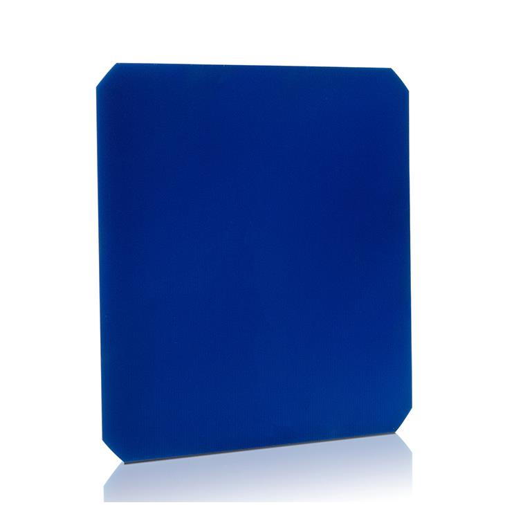
N Type IBC Solar Cell

In the interdigitated back contact (IBC) cell structure the emitter and contact are both on the back side of the wafer which allows independent optimization of the front surface for optical properties and back surface for electronic properties of the emitter and contacts. IBC solar cells have shown outstanding performance either on concentration or one-sun illumination. The advantages of this design include that there is no contact grid shading at the sunward side and potentially low substrate cost due to a thin device design. Moreover, the module assembling costs are potentially lower as both contacts are on the rear. Finally, the solar cells can be placed closer together in the module because there is no need for a space between the cells. Interdigitated Back Contact(IBC) solar cell is the key solution to the challenge of increasing cell efficiency and lowering the cost of solar cell manufacturing in solar cell industries.
【Product description】
N-type Mono bifacial PERT (passivated emitter rear totally diffused) silicon solar cells possesses high and stabilized conversion efficiencies.
N-type silicon solar cells are considered as promising alternatives to p-type solar cells for next generation highly efficient solar cells thanks to their ability to withstand light-induced degradation and to their higher tolerance to common metal impurities.
The n type bifacial PERT solar cell can be manufactured with process flow by using ion implant for single-sided doping for excellent emitter junction quality and uniformity, a single thermal anneal, integrated AlOx/ SiNx passivation layer and screen printed Ag grid on front and rear.

【Process flow】

【Key features】
High conversion efficiency with high reliability
No light-induced degradation
Uniform cell performance with stable process control
Both sides can generate electricity
Excellent power generation performance under low irradiation
Low hot spot risk
【Technical Data】
TECHNICAL DATA AND DESIGN | TEMPERATURE COEFFICIENTS AND SOLDERABILITY | |||
Dimension | 158.75mm*158.75mm±0.25 | TkUoc (%/K) | -0.302 | |
Thickness | 190±30 μm | TkIsc (%/K) | +0.048 | |
Front | 9 Busbars | TkPMAX (%/K) | -0.38 | |
Back | 9 Busbars | Peel Strength Minimum | >1.4N/mm | |
ELECTRICAL PARAMETERS at STC | |||||
No. | Efficiency (%) | Pmpp (W) | Uoc (V) | Isc (A) | FF (%) |
1 | 23.00% | 5.75 | 0.700 | 10.110 | 81.28 |
2 | 22.90% | 5.73 | 0.699 | 10.098 | 81.19 |
3 | 22.80% | 5.70 | 0.698 | 10.070 | 81.13 |
4 | 22.70% | 5.68 | 0.697 | 10.063 | 81.02 |
5 | 22.60% | 5.65 | 0.696 | 10.045 | 80.86 |
6 | 22.50% | 5.63 | 0.695 | 10.031 | 80.78 |
7 | 22.40% | 5.60 | 0.694 | 10.011 | 80.64 |
8 | 22.30% | 5.58 | 0.693 | 10.000 | 80.55 |
9 | 22.20% | 5.55 | 0.692 | 9.986 | 80.40 |
10 | 22.10% | 5.53 | 0.691 | 9.979 | 80.24 |
11 | 22.00% | 5.50 | 0.690 | 9.961 | 80.07 |
12 | 21.90% | 5.48 | 0.689 | 9.951 | 79.96 |
13 | 21.80% | 5.45 | 0.688 | 9.933 | 79.82 |
14 | 21.70% | 5.43 | 0.687 | 9.914 | 79.78 |
15 | 21.60% | 5.40 | 0.686 | 9.895 | 79.62 |
16 | 21.50% | 5.38 | 0.685 | 9.875 | 79.58 |
17 | 21.40% | 5.35 | 0.684 | 9.856 | 79.42 |
18 | 21.30% | 5.33 | 0.683 | 9.844 | 79.34 |
19 | 21.20% | 5.30 | 0.682 | 9.818 | 79.22 |
20 | 21.10% | 5.28 | 0.681 | 9.800 | 79.18 |
21 | 21.00% | 5.25 | 0.680 | 9.775 | 79.08 |

