Smile, Smart, Speed
고객의 만족을 위하여 최선을 다하는 기업, 정문사이언스입니다.

고객의 만족을 위하여 최선을 다하는 기업, 정문사이언스입니다.
 HOME > 회사소개 >소재 및 부속품
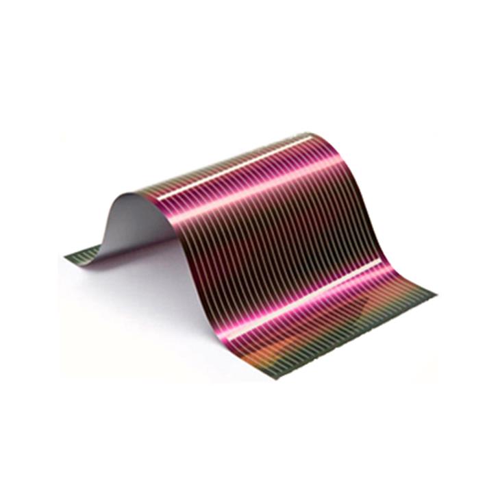
CIGS Copper Indium Gallium Diselenide Solar Cell
【Product description】
Thin-film PV, in particular CIGS, is a key technology to be one of the future technologies of photovoltaics and has great potential for further technological developments. CIGS thin-film modules have more and more investment in the solar industry.
As technology advancing it was later found that by substituting gallium (Ga) for indium (In), the bandgap can be increased from about 1.04 electron-volts (eV) for copper indium diselenide (CIS) films to about 1.68 eV for copper gallium diselenide (CGS) films. Optimal devices have been fabricated with only a partial substitution of Ga for In, leading to a substantial increase in overall efficiency and more optimal bandgap. These solar cells are commonly known as a copper indium gallium diselenide [Cu(InxGa1-x)Se2], or CIGS, cells.
The benefits of CIGS solar cells include:
High absorption: This direct-bandgap material can absorb a significant portion of the solar spectrum, enabling it to achieve the highest efficiency of any thin-film technology.
Tandem design: A tunable bandgap allows the possibility of tandem CIGS devices.
Protective buffer layer: The grain boundaries form an inherent buffer layer, preventing surface recombination and allowing for films with grain sizes of less than 1 micrometer to be used in device fabrication.

【Process flow】
Co-evaporation example | Alternatives |
Glass: 2mm or 3.2mm Stainless foil: 25um | Aluminum polyimide |
Molybdenum sputter, 0.3-1um Barrier layers: Cr/Nitride | Na barrier / Se barrier / Oxide barrier |
CIGS: 1stage / 2stage / 3stage Cu, In, Ga are co-evaporated in Se overpressure CIGS 1-2um | CIGS: Reactive sputtering, Ink deposition / Coating, Selenization, Co-evaporation |
Buffer layer: Chemical bath Deposition (CBD) CdS, 20-80nm | Buffer layer: Chemical bath deposition(CBD) / sputter; Zn(O,S): 20-80nm; |
Window layer: Sputter Resistive: i-ZnO, 0.1-0.12um Conductive: AZO, 0.1-0.15um | Window layer: MoCVD ZnO:B; InZnO; ITO |
Grids: evaporation Ni(150-500A) , Ag(500-6000A) Al (2-3um) | Grids / Screen print / Wire Overlay / Tab and string Interconnects |
【Key features】
No light induced degradation
Total area efficiency of up to 18%
Thiciness of thin to 0.33mm
Lightweight of lower to 7.5 gm
Ideal for many specialized uses.
Able to be modified to suit various applications.
Bendable and flexible
【Technical Data】
TECHNICAL DATA AND DESIGN | TEMPERATURE COEFFICIENTS AND SOLDERABILITY | |||
Length | 312mm+2/-4mm | TkUoc (%/K) | -0.28 | |
Width | 43.75mm±0.005mm | TkIsc (%/K) | +0.008 | |
Thickness | 0.33mm±0.1mm | TkPMAX (%/K) | -0.379 | |
Cell type | Copper Indium Gallium Diselenide | Peel Strength Minimum | >1.4N/mm | |
ELECTRICAL PARAMETERS at STC | |||||||
No. | Efficiency (%) | Pmpp (W) | Uoc (V) | Isc (A) | Vmpp (V) | Impp (A) | FF (%) |
1 | 18.00% | 2.45 | 0.681 | 4.7 | 0.561 | 4.37 | 76.59% |
2 | 17.50% | 2.38 | 0.676 | 4.7 | 0.552 | 4.31 | 74.88% |
3 | 17.00% | 2.32 | 0.673 | 4.7 | 0.545 | 4.25 | 73.23% |
4 | 16.50% | 2.25 | 0.670 | 4.7 | 0.538 | 4.17 | 71.24% |
5 | 16.00% | 2.18 | 0.664 | 4.7 | 0.531 | 4.11 | 69.93% |
6 | 15.50% | 2.12 | 0.661 | 4.7 | 0.526 | 4.04 | 68.40% |
7 | 15.00% | 2.06 | 0.658 | 4.7 | 0.521 | 3.97 | 66.88% |
8 | 14.50% | 2.01 | 0.655 | 4.7 | 0.516 | 3.90 | 65.37% |

