Smile, Smart, Speed
고객의 만족을 위하여 최선을 다하는 기업, 정문사이언스입니다.

고객의 만족을 위하여 최선을 다하는 기업, 정문사이언스입니다.
 HOME > 회사소개 >소재 및 부속품
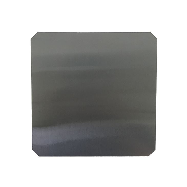
P Type Monocrystalline Solar Wafer
M4 P-type monocrystalline wafer is 161.7mm x 161.7mm.
![]()


1 Material properties
Property | Specification | Inspection Method |
Growth method | CZ | |
Crystallinity | Monocrystalline
| Preferential Etch Techniques(ASTM F47-88) |
Conductivity type | P-type | Napson EC-80TPN P/N |
Dopant
| Boron
| - |
Oxygen concentration[Oi] | ≦8E+17 at/cm3 | FTIR (ASTM F121-83) |
Carbon concentration[Cs] | ≦5E+16 at/cm3 | FTIR (ASTM F123-91) |
Etch pit density(dislocation density) | ≦500 cm-3 | Preferential Etch Techniques(ASTM F47-88) |
Surface orientation | <100>±3° | X-ray Diffraction Method (ASTM F26-1987) |
Orientation of pseudo square sides | <010>,<001>±3° | X-ray Diffraction Method (ASTM F26-1987) |
2 Electrical properties
Property | Specification | Inspection Method |
Resistivity | 0.5-1.5 Ωcm | Wafer inspection system |
MCLT (minority carrier lifetime) | ≧50 μs | Sinton BCT-400 (with injection level: 1E15 cm-3) |
3 Geometry
Property | Specification | Inspection Method |
Geometry | Quasi square | |
Wafer Side length | 161.7±0.25 mm | wafer inspection system |
Wafer Diameter | φ221±0.25 mm | wafer inspection system |
Angle between adjacent sides | 90° ± 0.2° | wafer inspection system |
Thickness | 180 ﹢ 20/﹣10 µm; 170﹢ 20/﹣10 µm | wafer inspection system |
TTV (Total thickness variation) | ≤ 27 µm | wafer inspection system |

4 Surface properties
Property | Specification | Inspection Method |
Cutting method | DW | -- |
Surface quality | as cut and cleaned, no visible contamination, (oil or grease, finger prints, soap stains, slurry stains, epoxy/glue stains are not allowed) | wafer inspection system |
Saw marks / steps | ≤ 15µm | wafer inspection system |
Bow | ≤ 40 µm | wafer inspection system |
Warp | ≤ 40 µm | wafer inspection system |
Chip | depth ≤0.3mm and length ≤ 0.5mm Max 2/pcs; no V-chip | Naked eyes or wafer inspection system |
Micro cracks / holes | Not allowed | wafer inspection system |

