Smile, Smart, Speed
고객의 만족을 위하여 최선을 다하는 기업, 정문사이언스입니다.

고객의 만족을 위하여 최선을 다하는 기업, 정문사이언스입니다.
 HOME > 회사소개 >소재 및 부속품
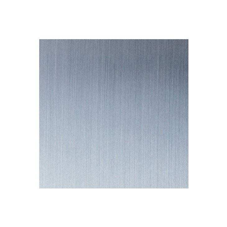
P Type Monocrystalline Solar Wafer


Currently silicon solar PV is mainly using 156.75mm x 156.75mm P-type monocrystalline wafers, but some the them are migrating to larger wafer and cell sizes such as 158.75mm x 158.75mm. Some of the manufacturers have already started that process. One of the reason for the 158.75mm square wafer getting more focus is that the close module dimensions to past standard 60-cell and 72-cell modules, providing retrofit and retention of existing manufacturing equipment.
In the future for mono-Si wafers, 158.75mm full square will become the most adopted design by most solar PV manufacturers. Of course there are a few manufacturers use wafers that are larger than this. LG and Hanwha Q Cells, for instance, use M4 wafers (161.7mm), while Longi is promoting 166mm(M6) wafers.
1 Material properties
Property | Specification | Inspection Method |
Growth method | CZ | |
Crystallinity | Monocrystalline
| Preferential Etch Techniques(ASTM F47-88) |
Conductivity type | P-type | Napson EC-80TPN P/N |
Dopant
| Boron
| - |
Oxygen concentration[Oi] | ≦8E+17 at/cm3 | FTIR (ASTM F121-83) |
Carbon concentration[Cs] | ≦5E+16 at/cm3 | FTIR (ASTM F123-91) |
Etch pit density(dislocation density) | ≦500 cm-3 | Preferential Etch Techniques(ASTM F47-88) |
Surface orientation | <100>±3° | X-ray Diffraction Method (ASTM F26-1987) |
Orientation of pseudo square sides | <010>,<001>±3° | X-ray Diffraction Method (ASTM F26-1987) |
2 Electrical properties
Property | Specification | Inspection Method |
Resistivity | 0.5-1.5 Ωcm | Wafer inspection system |
MCLT (minority carrier lifetime) | ≧50 μs | Sinton BCT-400 (with injection level: 1E15 cm-3) |
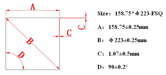
3 Geometry
Property | Specification | Inspection Method |
Geometry | Full square | |
Wafer Side length | 158.75±0.25 mm | wafer inspection system |
Wafer Diameter | φ223±0.25 mm | wafer inspection system |
Angle between adjacent sides | 90° ± 0.2° | wafer inspection system |
Thickness | 180 ﹢ 20/﹣10 µm; 170﹢ 20/﹣10 µm | wafer inspection system |
TTV (Total thickness variation) | ≤ 27 µm | wafer inspection system |
4 Surface properties
Property | Specification | Inspection Method |
Cutting method | DW | -- |
Surface quality | as cut and cleaned, no visible contamination, (oil or grease, finger prints, soap stains, slurry stains, epoxy/glue stains are not allowed) | wafer inspection system |
Saw marks / steps | ≤ 15µm | wafer inspection system |
Bow | ≤ 40 µm | wafer inspection system |
Warp | ≤ 40 µm | wafer inspection system |
Chip | depth ≤0.3mm and length ≤ 0.5mm Max 2/pcs; no V-chip | Naked eyes or wafer inspection system |
Micro cracks / holes | Not allowed | wafer inspection system |

