Smile, Smart, Speed
고객의 만족을 위하여 최선을 다하는 기업, 정문사이언스입니다.

고객의 만족을 위하여 최선을 다하는 기업, 정문사이언스입니다.
 HOME > 회사소개 >소재 및 부속품
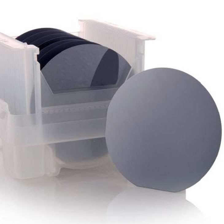
8 Inch (200mm) Wafer
【Product introduction】
 Polished Wafer DSC01147 730")
 Polished Wafer DSC01144 730")
Parameter | Characteristic | ASTM Control Method |
Type/Dopant | P, Boron N, Phosphorous N, Antimony N, Arsenic | F42 |
Orientations | <100>, <111> slice off orientations per customer's specifications | F26 |
Oxygen Content | 1019 ppmA Custom tolerances per customer's specification | F121 |
Carbon Content | < 0.6 ppmA | F123 |
Resistivity ranges- P, Boron- N, Phosphorous- N, Antimony- N, Arsenic | 0.001 - 50 ohm cm | F84 |
Parameter | Prime | Monitor/ Test A | Test | ASTM Method |
Diameter | 200 ± 0.2 mm | 200 ± 0.2 mm | 200 ± 0.5 mm | F613 |
Thickness | 725 ± 20 µm (standard) | 725 ± 25 µm (standard) 450 ± 25 µm 625 ± 25 µm 1000 ± 25 µm 1300 ± 25 µm 1500 ± 25 µm | 725 ± 50 µm (standard) | F533 |
TTV | < 5 µm | < 10 µm | < 15 µm | F657 |
Bow | < 30 µm | < 30 µm | < 50 µm | F657 |
Wrap | < 30 µm | < 30 µm | < 50 µm | F657 |
Edge Rounding | SEMI-STD | F928 | ||
Marking | Primary SEMI-Flat only, SEMI-STD Flats Jeida Flat, Notch | F26, F671 | ||
Parameter | Prime | Monitor/ Test A | Test | ASTM Method |
Front Side Criteria | ||||
Surface condition | Chemical Mechanical Polished | Chemical Mechanical Polished | Chemical Mechanical Polished | F523 |
Surface Roughness | < 2 A° | < 2 A° | < 2 A° | |
Contamination,Particles @ >0.3 µm | = 20 | = 20 | = 30 | F523 |
Haze, Pits, Orange peel | None | None | None | F523 |
Saw Marks, striations | None | None | None | F523 |
Back Side Criteria | ||||
Cracks, crowsfeet, saw marks,stains | None | None | None | F523 |
Surface condition | Caustic etched | F523 | ||
【Product description】
Perfect for microfluidics applications. For microelectronics or MEMS applications, please contact us for detailed specs.
Microelectronics’ product line includes both single side polished (SSP) and double side polished (DSP) wafer substrates. Double side polished wafers are typically required in semiconductor, MEMS, and other applications where wafers with tightly controlled flatness characteristics are required. They are also needed for double side patterning and device manufacturing projects.
Large stock of double side polished wafers in all wafer diameters ranging from 100mm to 300mm. If your specification is not available in our inventory, we have established long term relationships with numerous vendors that are capable of custom manufacturing wafers to fit any unique specifications. Double side polished wafers are available in silicon, glass and other materials commonly used in the semiconductor industry.
Customized dicing and polishing is also avaible according to your requirements. Please feel free to contact us.
【Product features】
· 8" P/N type, Polished silicon wafer (25 pcs)
· Orientation: 200
· Resistivity: 0.1 - 40 ohm•cm (It may vary from batch to batch)
· Thickness: 725+/-20um
· Prime/Monitor/Test Grade

