Smile, Smart, Speed
고객의 만족을 위하여 최선을 다하는 기업, 정문사이언스입니다.

고객의 만족을 위하여 최선을 다하는 기업, 정문사이언스입니다.
 HOME > 회사소개 >소재 및 부속품
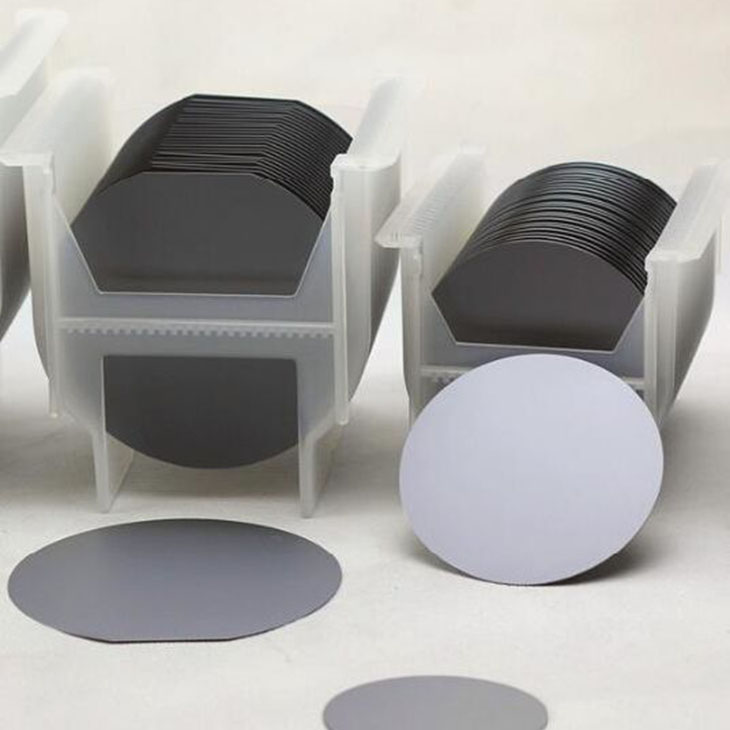
4 Inch (100mm) Wafer
【Product introduction】


MATERIAL PROPERTIES
Parameter | Characteristic | ASTM Control Method |
Type/Dopant | P, Boron N, Phosphorous N, Antimony N, Arsenic | F42 |
Orientations | <100>, <111> slice off orientations per customer's specifications | F26 |
Oxygen Content | 1018 ppmA Custom tolerances per customer's specification | F121 |
Carbon Content | < 0.5 ppmA Custom tolerances per customer's specification | F123 |
Resistivity ranges- P, Boron- N, Phosphorous- N, Antimony- N, Arsenic | 0.001 - 50 ohm·cm | F84 |
MECHANICAL PROPERTIES
Parameter | Prime | Monitor/ Test A | Test | ASTM Method |
Diameter | 100 ± 0.2 mm | 100 ± 0.2 mm | 100 ± 0.5 mm | F613 |
Thickness | 525 ± 20 µm (standard) | 525 ± 25 µm (standard) 381 ± 25 µm 625 ± 25 µm 700 ± 25 µm 800 ± 25 µm 1000 ± 25 µm 1500 ± 25 µm | 525 ± 50 µm (standard) | F533 |
TTV | < 5 µm | < 10 µm | < 15 µm | F657 |
Bow | < 30 µm | < 30 µm | < 40 µm | F657 |
Wrap | < 30 µm | < 30 µm | < 40 µm | F657 |
Edge Rounding | SEMI-STD | F928 | ||
Marking | SEMI-STD Flats, Primary SEMI-Flat only | F26, F671 | ||
SURFACE QUALITY
Parameter | Prime | Monitor/ Test A | Test | ASTM Method |
Front Side Criteria | ||||
Surface condition | Chemical Mechanical Polished | Chemical Mechanical Polished | Chemical Mechanical Polished | F523 |
Surface Roughness | < 2 A° | < 2 A° | < 2 A° | |
Contamination,Particles @ >0.3 µm | = 20 | = 20 | = 30 | F523 |
Haze, Pits, Orange peel | None | None | None | F523 |
Saw Marks, striations | None | None | None | F523 |
Back Side Criteria | ||||
Cracks, crowsfeet, saw marks,stains | None | None | None | F523 |
Surface condition | Caustic etched | F523 | ||
【Product description】
Microelectronics’ product line includes both single side polished (SSP) and double side polished (DSP) wafer substrates. Double side polished wafers are typically required in semiconductor, MEMS, and other applications where wafers with tightly controlled flatness characteristics are required.
We also offer rectangular and square wafer pieces. Basically realisable range of the edge lengths for silicon wafers is 5 x 5 mm2 ... 100 x 120 mm2 etc. The cost / wafer piece depends on the material as well as on the number of wafer pieces required.
Customized dicing and polishing is also avaible according to your requirements. Please feel free to contact us.
【Product features】
· 4" P/N type, Polished silicon wafer (25 pcs)
· Orientation: 100
· Resistivity: 0.1 - 40 Ohm·cm (It may vary from batch to batch)
· Thickness: 525+/-20um
· Prime/Monitor/Test Grade

