Smile, Smart, Speed
고객의 만족을 위하여 최선을 다하는 기업, 정문사이언스입니다.

고객의 만족을 위하여 최선을 다하는 기업, 정문사이언스입니다.
 HOME > 회사소개 >
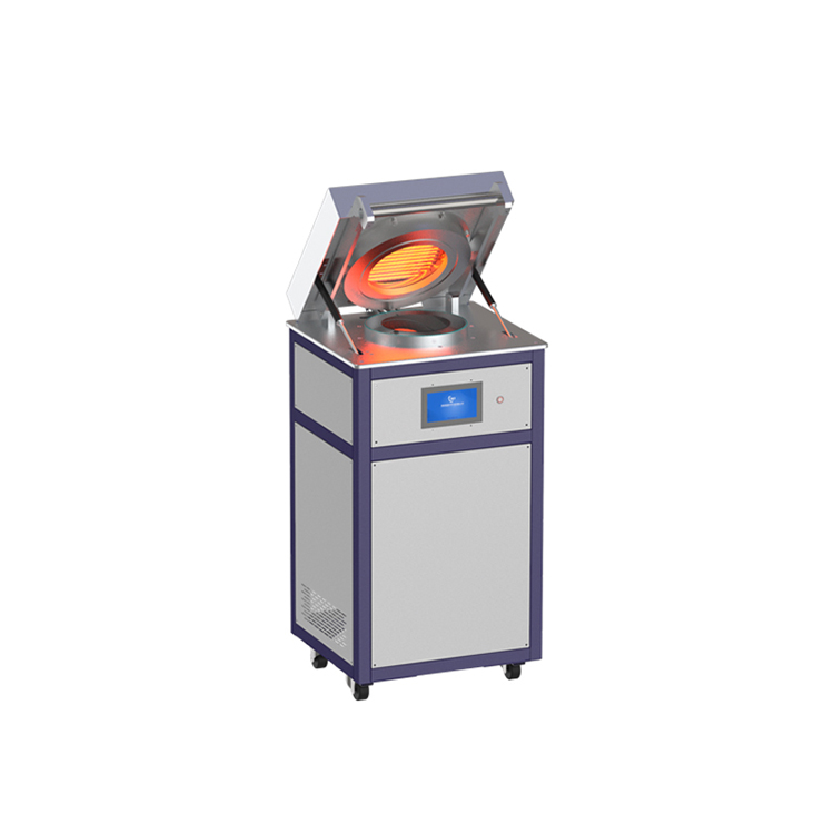
Halogen lamp RTP annealing furnace


The halogen lamp RTP annealing furnace is a
6-inch wafer rapid annealing furnace. It adopts innovative heating technology
to realize real substrate temperature measurement. It does not need the
temperature compensation of traditional rapid annealing furnaces. The
temperature control is accurate and the temperature is highly repeatable.
Customers include many international semiconductor companies and well-known
scientific research teams. It is an ideal choice for semiconductor annealing
process.
Technical features:
Real substrate temperature measurement
without traditional temperature compensation
Infrared halogen tube lamp heating
Extremely excellent heating temperature
accuracy and uniformity
Fast digital PID temperature control
Stainless steel cold wall vacuum chamber
Good system stability
Compact structure, small desktop system
PC control with touch screen
Compatible with normal pressure and vacuum
environment, the standard value of vacuum degree is 5×10⁻³ Torr, and the vacuum
degree is as low as 5×10⁻⁶ Torr using two-stage molecular pump
Up to 3-channel gases (MFC control)
No cross contamination, no metal
contamination.
As shown in the figure above, the heat
radiated by the array halogen lamp reaches the surface of the sample through
the quartz window, and the sample is heated. The traditional rapid annealing
furnace uses a thermocouple to measure the substrate temperature. Because the
thermocouple is at a certain distance from the substrate, the measurement is
not the substrate. The real temperature of the chip must be temperature
compensated.
The halogen lamp RTP annealing furnace uses
a dedicated flake-like Real T/C KIT for temperature measurement, as shown in
the figure above, the contact thermometer is connected to the flake-like Real
T/C KIT. The flake-like Real T/C KIT is located very close to the sample above
when working, the array halogen lamp radiates heat to the sample surface
through the quartz window, the sample is heated, and the flake-like Real T/C
KIT is heated at the same time. Because the substrate is very close to the Real
T/C KIT, there will be heat transfer between them, and the thermal equilibrium
will be quickly reached, so the temperature measured by the flake-like Real T/C
KIT is infinitely close to the real temperature of the substrate, thus
realizing the real measurement of the substrate temperature.
Technical parameters:
|
Substrate size |
6 inches |
|
Substrate base |
Quartz needle (optional SiC coated
graphite base) |
|
Temperature range |
150-1250℃ |
|
Heating rate |
10-150℃/S |
|
Temperature uniformity |
≤±1.5% (@800℃, Silicon wafer) ≤±1.0% (@800℃, Substrate on SiC coated
graphite susceptor) |
|
Temperature control accuracy |
≤ ±3℃ |
|
Temperature repeatability |
≤ ±3℃ |
|
Vacuum |
5.0E-3 Torr / 5.0E-6 Torr |
|
Gas supply |
Standard 1 channel N2 purge and cooling
gas circuit, controlled by MFC (up to 3 channels can be selected) |
|
Annealing duration |
≥35min@1250℃ |
|
Temperature control |
Fast digital PID control |
|
Dimensions |
870mm*650mm*620mm |
Substrate type:
• Silicon wafers
• Compound semiconductor wafers
• GaN/Sapphire wafers for LEDs
• Silicon carbide wafers
• Poly silicon wafers for solar cells
• Glass substrates
• Metals
• Polymers
• Graphite and silicon carbide
susceptors
Application areas:
Ion implantation/contact annealing, rapid
thermal processing (RTP), rapid annealing (RTA), rapid thermal oxidation (RTO),
rapid thermal nitridation (RTN), can be used in different environments such as
vacuum, inert atmosphere, oxygen, hydrogen, mixed gas, etc. SiAu, SiAl, SiMo
alloying, low dielectric materials, crystallization, densification, solar cell
bonding, etc.

